
SEH has the largest portfolio of silicon products
available in the industry.


POLISHED CZ
SEH can offer polished wafers manufactured with standard CZ crystal technology. The 200MM polishing process can be optimized to meet the flatness requirements of leading edge design rules ( to 90nm or below ).
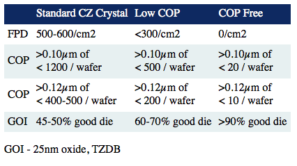
Standard CZ technology suffers from the problem of high COP levels. Vacancy related crystal defects such as COP/FPD (Crystal Originated Pits/Flow Pattern Defects) can cause near surface problems during device manufacture. Examples of the device problems associated with these defects are poor GOI (TZDB, TDDB) and current leakage in P-N Junctions. COPs are 0.1-0.2µm octahedral shaped voids with walls covered by oxide. FPD is a vacancy cluster related defect exposed by preferential etching.
The general trend is that standard CZ wafers are appropriate for design technologies greater than 180nm, while more advanced technologies are generally considered at 180nm design rules and below.
See also our Epi, Annealed Wafer and Low Defect Crystal offerings.
POLISHED WAFER: LOW COP/COP FREE
Vacancy related crystal defects such as COP/FPD (Crystal Originated Pits/Flow Pattern Defects) can cause near surface problems during device manufacture. Examples of the device problems are poor GOI and current leakage in P-N Junctions. COPs are 0.1-0.2um octahedral shaped voids with walls covered by oxide. FPD is a vacancy cluster related defect exposed by preferential etching. Adding an epitaxial layer can eliminate these defects, although epi growth adds costs. For some device applications, a low defect crystal growth method can be applied to reduce the number of vacancy defects in the near surface device region. Modification of the crystal pulling speed and the cooling rate of the crystal can result in lower vacancy defect levels. This allows for the recombination between vacancies and interstitials, vacancy agglomeration and oxygen control resulting in reduction of surface defects.
SEH is able to provide two different levels of surface defect reduction: Low Defect Crystal and Near Perfect, COP Free Crystal. Both of these products provide a significant reduction in surface defects when compared to the standard CZ crystal. SEH produces near Epi surface quality in a FPD/COP free Polished Wafer with our NPC wafer.
SEH CZ Crystals can provide the following quality levels:
With the arrival of the era of full-scale mass production of 300mm wafers, customers’ expectations of silicon wafers are increasingly high. As a pioneer in the world silicon market, Shin-Etsu Handotai (SEH) took the head start of the mass production of 300mm and has established a system ensuring a stable supply to the market.
In responding to even higher requirements from the customers for the future, we continue the incessant efforts and challenges for the quality improvements.
Features – 300mm silicon wafers
We have responded to the growing market demand in a timely manner with our capacity expansions since the starting of the mass production in February 2001.
Our products can meet the 20-22 nm design rule process and beyond.
Our product portfolio covers a wide range of our customers’ various requirements.
Applications
Substrates for memory devices, microprocessor devices, etc.
Product Data
Overview
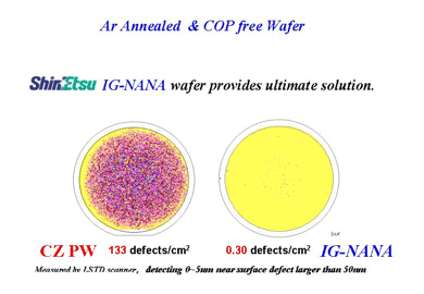
In today’s advanced device applications, near surface defects such as COP’s and oxygen precipitates have caused degraded device yield and performance. It has been common practice to form bulk micro defects during device processing by carefully structuring device thermal processes around material bulk micro defect formation primarily through oxygen precipitation. However, with the present day’s movement toward lower thermal budgets it is more costly to do so.
SEH provides IG NANA™, nitrogen doped, and argon annealed.
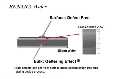
SEH IG NANA™ (Nitrogen Assisted Nucleate Acceleration) material provides the best starting material for those applications that benefit from a defect- free near surface and a high density of bulk micro defects to provide high intrinsic gettering efficiency from initial oxidation through device completion. IG NANA™ can provide cost benefits through yield enhancement and process simplification.
- Near surface region is free of COP and oxygen precipitations
- Superior GOI Denuded zone depth tailored to specific application.
- Bulk Micro Defects (BMD) >= 1e9/cm3 uniform edge to edge
- Low slip level Benefits
Benefits
IG NANA™ has provided our customers a more robust device process resulting in increased device yields and lowered manufacturing costs. IG NANA™ is one of SEH’s most popular products with further growth being seen in sub .18um technologies including Flash memory, DRAMs, M/ROMS, SRAMS, and other logic devices. IG NANA™ has also been optimized for higher voltage devices which typically require resistivity of 50 to 200 ?-cm and operate with depletion regions of 50 to 100 microns.
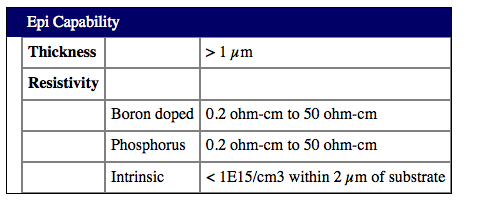
P/P+ AND P/P- | N/N+ | EPI NANA™ (Nitrogen Doping + EPI) | Intrinsic EPI | EPI Wafers for Image Sensors
P/P+ AND P/P-
SEH is a world leader in epitaxial silicon technology. Our tool set, recipe development and process control systems are capable of delivering a very high quality epi wafer for your applications.
Epi wafers for CMOS applications are available in diameters up to 300mm and for Discrete/Power applications up to 200mm diameter.
For CMOS image sensors and CCD, special EPI wafers are available with very low metallic impurities and µ-PCD lifetime > 1000 µ-sec
N/N+ – EPI WAFERS FOR DISCRETE DEVICES
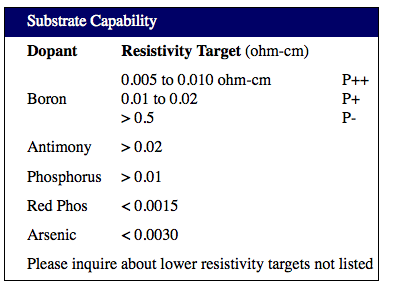
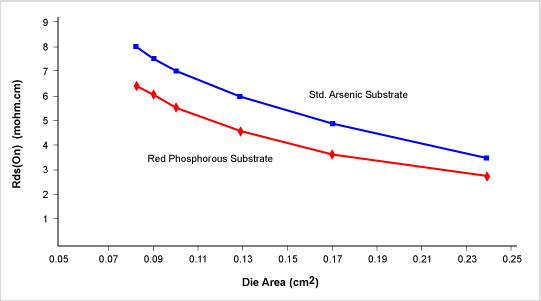
SEH can provide epi wafers specifically for discrete, bipolar and power MOSFET applications. Combinations of n-type and p-type epi layers and substrates are available for these device applications. N+ substrates can be doped with phosphorus, antimony, arsenic. Red phosphorus substrates are available for Power MOSFET applications requiring very heavy doping to minimize Rds(On)*.
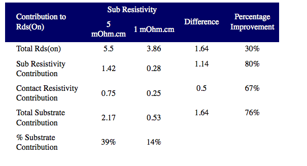
The performance of MOSFET and/or the Schottkey rectifiers used in VRM’s (Voltage Regulated Modules) is extremely dependent on the voltage drop across these devices, making the substrate resistivity of paramount importance. Achieving low Rds(On) by reducing substrate resistivity can eliminate the need to develop the next technology platform, and thus reduce cost and time to market.
Improvement of 20V Power MOSFET by Low Substrate Resistivity
Improvement of Rds(On) by Low Resistivity Substrate as a Function of Die Size
Premium N-Type Substrate Capabilities: Resistivity in mOhm.cm
Very heavily doped boron substrates < 0.005 ohm-cm are also available.
Thick epi films are available for high voltage applications and tight epi thickness and resistivity uniformity is available to control variation within wafer and from wafer-to-wafer. SEH takes advantage of the superior capabilities of single wafer epi reactors to meet the specifications required for this market segment. Epi films can be doped with phosphorus or boron.
Wafers with two or three epi layers are also available for IGBT and other applications.
* Rds(on) is the resistance between the drain and source of a forward-biased power MOSFET at a specified drain current and gate voltage.
EPI NANA™ (NITROGEN DOPING + EPI)
Utilizing our patented nitrogen doping technology, SEH offers a P/P- epi wafer optimized for low temperature advanced CMOS devices. The P- lightly doped substrate includes levels of nitrogen optimized to enhance oxygen precipitation. In standard P/P- epi wafers without nitrogen doped substrates, the oxygen precipitate nuclei are annihilated during the epi layer growth. For this reason, standard P/P- epi wafers typically have poor metal gettering characteristics and are also susceptible to slip and other problems associated with low mechanical strength.
The enhanced precipitation created by the nitrogen doped substrate adds gettering ability from the beginning of the fab process, and also increases resistance to slip during high temperature processes such as epi and RTA.
EPI NANA™ wafers are available in both 200mm and 300mm diameters and are used world-wide for leading edge design rule processes. > 1000 µ-sec
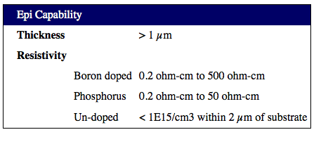
INTRINSIC EPI
SEH is a world leader in epitaxial silicon technology. Our tool set, recipe development and process control systems are capable of delivering a very high quality epi wafer for your applications. Epi wafers for CMOS applications are available in diameters up to 300mm and for Discrete/Power applications up to 200mm diameter. Intrinsic or un-doped EPI wafers are available. Our process is capable of achieving carrier concentrations <1E13/cm3 in layers > 5 microns. Very lightly doped EPI layers with targeted resistivity in the 100 to 500 ?-cm range are also available.

EPI Wafers for Image Sensors
SEH offers several epi products suitable for image sensor manufacture. Image sensors are most commonly manufactured on epi wafers. CMOS and CCD image sensors have in common two requirements important in the selection of a silicon starting material. First, the surface quality must be very high, with few defects which might impair the function of one of more pixels. Second, the dark current must be low for good signal to noise performance, and this means that metallic impurities responsible for forming recombination centers must be very low in the surface region. The silicon wafer is selected to effectively getter these metallic impurities.
SEH has the epi experience to produce very low defect densities in an epi layer. Stacking faults and other epi defects are minimized through effective substrate cleaning and effective reactor defect controls. Sensitive laser scattering inspection equipment is used to guarantee the surface quality of epi layers, complemented by visual inspection techniques.
SEH has several approaches to effective gettering for image sensor devices;
P/P+ or N/N+
P/P- on N/N- with enhanced gettering
Heavily doped p-type substrates provide effective gettering for Fe, Cu, and Ni impurities. Several proprietary gettering enhancement techniques for P/P- and N/N- wafers are also available, utilizing nitrogen doping and additional thermal treatments to enhance oxygen precipitation.
SEH also can provide analytical techniques to determine what metallic impurities and process defects are increasing dark current levels. From this analysis, we can recommend the most effective silicon substrate solution.
SOI wafers are commonly used semiconductor materials for leading edge devices such as low power and high speed LSI’s, smart sensors, MEMS, and smart power devices. SEH has been providing several kinds of SOI wafers to meet various customers’ requirements.
SEH started development of SOI wafers in 1988. We began with bonded SOI wafers by precisely controlled grinding and polishing technology, responding to customers’ high quality requirements. We introduced Unibond® technology for thin SOI wafer production at low cost in 1997.
To meet customer demands for SOI layers in the 1.0 to 5.0 µm thickness range with excellent uniformity within wafer and wafer-to-wafer, SEH has optimized EPI growth on Unibond® SOI wafers. EPI on SOI can also be used to produce SOI stacks of dissimilar dopants and resistivity.
SOI Products from SEH:
Thick SOI Wafer (Bonded and Polished SOI with layer thickness > 1µm) Thin SOI Wafers (Unibond® SOI with layer thickness < 1µm)
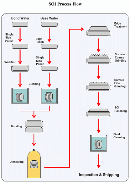
Thick SOI Wafer
SEH has a long history of SOI production. Our SOI facility in Nagano was established in 1988, and a new facility was built in 1997 to provide adequate capacity to support semiconductor customers and the developing micro-technology industry through at least 2010. SEH has the world’s largest capacity for production of thick bonded SOI wafers, and we currently supply more than 50% of the SOI wafers used for semiconductor, MEMS, and MOEMS applications.
SEH’s bonding and polishing process is similar to that being used by several other SOI manufacturers, but SEH has designed and developed it’s own fabrication equipment that can produce the highest quality wafers for even the most demanding applications. SEH thick bonded SOI wafers feature a 0.8 mm edge terrace width that increases the chip yield on a wafer by up to 5% for a 5mm x 5 mm device.
A large inventory of finished SOI products is always available for customers who have an immediate need for research and development material, but our real strength lies in our ability to custom design SOI wafers for any customers needs. SEH’s expertise as a manufacturer of low defect, annealed, or high resistivity crystal means that we can produce SOI wafers built with crystal that is also custom designed for the customer’s application.
Optional ion implanted buried layers and the capability to manufacture multiple active layer structures make SEH the obvious choice for anyone looking for the latest technology and highest quality SOI wafers.
Thin SOI Wafer
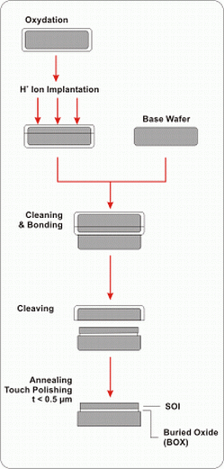
Although SEH’s thick bonding and polishing process produces wafers that are suitable for many semiconductor and MEMS applications, the limits of the polishing technology created a need for another process that could produce even thinner layers with even tighter layer thickness uniformity. SEH also offers a thin SOI Unibond® wafer manufactured with the SmartCut® process, which is licensed from Soitec.
In the thin bonding process, the active and handle wafers are bonded as in the thick bonding process, but the active wafer includes a hydrogen implanted layer. After bonding, the SOI wafer is annealed at moderate temperatures after which the bulk of the active layer separates from the bonded portion at the limit of the hydrogen implant. (See Figure 1.) Minimal additional processing is required to produce the final SOI wafer.
The SOI wafers produced by this process have very thin active layers with exceptional layer thickness uniformity. Thickness of 1000 nm and below are possible with a uniformity of <±5%. These wafers are of the highest quality with HF and Secco defect concentrations that are suitable for the most demanding semiconductor applications.
SEH’s Unibond® process is now available for 200 mm and 300 mm wafers. Our new facility in Yokonodaira, Japan has adequate capacity to meet the needs of the semiconductor industry for the foreseeable future.
HIGH RESISTIVITY CA CRYSTAL FOR RF SOC APPLICATIONS
The integration of RF circuits into CMOS devices favors a shift to a very high silicon substrate resistivity. RF circuitry requires linear, analog devices with low noise and precision passive components (e.g., resistors, capacitors and inductors). Very high substrate resistivity decreases capacitively-coupled cross-talk between digital, analog and RF components, improving noise isolation. High- res silicon also improves the quality factor of spiral inductors by decreasing eddy current losses.
Float Zone crystal has typically been the only silicon option for applications requiring a resistivity greater than 1,000 ohm.cm, but FZ crystal is not currently readily available at 200/300mm. SEH has now developed and patented several techniques to manufacture CZ crystal with a resitivity of greater than 1,000 ohm.cm, and these wafers are available in production quantities today. (U.S. patent 6,544,656B1)
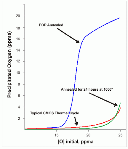
The main issue in High Res CZ is the management of Oi. High levels of Oi lead to thermal donor generation which creates unstable resistivity in the temperature range 350°c to 500°c common in back-end processes.
Oi must be reduced by special prescription thermal cycles (ref. U.S. patent #6,544,656) or the Oi level must be kept low by MCZ pulling processes
LOW OI MCZ
The CZ ingot growing process uses a fused quartz crucible to contain the silicon melt as the crystal is pulled from the melt over a period of up to 36 hours. Although structurally stable, this quartz crucible slowly devitrifies and dissolves during the course of the crystal’s growth, liberating oxygen into the silicon melt and resulting in the oxygen concentration that characterizes CZ silicon. Control of crucible rotations and the environment within the crystal growing furnace has allowed engineers to minimize the oxygen concentration of CZ grown crystal but, until the advent of the magnetic CZ (MCZ) process, there have been very practical limits on the extent of such controls.
In the MCZ process, a super conducting magnet sits alongside of the crystal growing furnace and generates a magnetic field that inhibits the turbulent thermal convection that conveys oxygen through the silicon melt. Crystal growing engineers can now use this magnetic field to significantly limit the incorporation of oxygen in the crystal and also to produce more uniform crystal by stabilizing the temperature at the melt-crystal interface. Essentially, the magnetic field increases the viscosity of the silicon melt.
Low Oi levels reduce the amount of oxygen related thermal donors which can degrade the resistivity of silicon. For specific applications in which the presence of the heavy precipitation associated with the High Res FOP is not desirable, low Oi MCZ silicon may be a good choice.
For most applications, low Oi high res MCZ wafers are proven to be superior to the high Oi + precipitation technique. MCZ wafers with Oi levels <6.4 ppma ASTM ’83 can provide performance very similar to FZ wafers
8 ppma SEH
↓
6.4 ppma A’80
Test Wafers with “Low COP” for fab particle monitoring
As design rules shrink below 180nm, most fab engineers are interested in the ability to monitor the particle additions of their process tools and related equipment to defect sizes far below the design rule. As a general rule of thumb for the critical defect size is 0.5x the design rule, it would be necessary to monitor defect additions at 90nm while running a device manufactured by 180nm design rules.
Historically, particle test wafers used for fabs have been grown by standard CZ techniques, which have resulted in high levels of COP ( crystal originated particles ). The COP typically have a physical size of 100-150nm, and are detected by laser scattering metrology equipment in the range of 80-120nm. The relatively high counts of COP on a 200mm wafer ( between 200 and 1000 COP per wafer ) make it more difficult to detect real fab defects while scanning these wafers.
Metrology equipment suppliers such as KLA-Tencor have created sophisticated algorithms to distinguish COP from “real” defects. While these techniques can be quite useful, it sometimes becomes necessary to use a “low COP” or “COP free” wafer as a particle test wafer.
SEH has several options for this application. This includes wafers processed from special COP free ingots, and also wafers manufactured with nitrogen doping. Nitrogen has the impact of dramatically reducing the size of COP in as-grown CZ silicon, and it is possible to reduce the size of the COP below the critical defect size of interest. For example, the COP density detectable at 90nm may be low enough that standard laser scattering techniques can detect very small shifts in “real” fab defects added.
Contact SEH with your specific fab particle monitoring requirements.
PHOTOLITHOGRAPHY
Fab lithography engineers frequently have a need to use silicon wafers with extremely tight flatness in order to complete maintenance and qualification testing on leading edge lithography tools such as steppers and scanners. This flatness requirement typically is described in global flatness terms such as TTV. SEH has extensive experience in meeting the special needs of this application.
Contact us with your special requirements.
N/N+
EPI WAFERS FOR DISCRETE DEVICES SEH can provide epi wafers specifically for discrete, bipolar and power MOSFET applications. Combinations of n-type and p-type epi layers and substrates are available for these device applications. N+ substrates can be doped with phosphorus, antimony, arsenic. Red phosphorus substrates are available for Power MOSFET applications requiring very heavy doping to minimize Rds(On)*.
The performance of MOSFET and/or the Schottkey rectifiers used in VRM’s (Voltage Regulated Modules) is extremely dependent on the voltage drop across these devices, making the substrate resistivity of paramount importance. Achieving low Rds(On) by reducing substrate resistivity can eliminate the need to develop the next technology platform, and thus reduce cost and time to market.
Improvement of 20V Power MOSFET by Low Substrate Resistivity
Improvement of Rds(On) by Low Resistivity Substrate as a Function of Die Size
Premium N-Type Substrate Capabilities: Resistivity in mOhm.cm
Very heavily doped boron substrates < 0.005 ohm-cm are also available.
Thick epi films are available for high voltage applications and tight epi thickness and resistivity uniformity is available to control variation within wafer and from wafer-to-wafer. SEH takes advantage of the superior capabilities of single wafer epi reactors to meet the specifications required for this market segment. Epi films can be doped with phosphorus or boron.
Wafers with two or three epi layers are also available for IGBT and other applications.
* Rds(on) is the resistance between the drain and source of a forward-biased power MOSFET at a specified drain current and gate voltage.
FLOAT ZONE WAFERS
Float Zone ( also Floating Zone or FZ ) wafers are used primarily for applications in which very high resistivity or the absence of oxygen are necessary for good device performance. Such applications include discrete power, MOS power, high efficiency solar cells and RF/wireless communication chips.
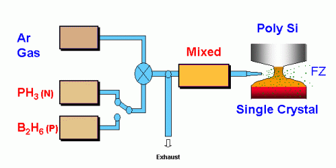
FZ wafers are sliced from ingots manufactured by the float zone process, in which a polycrystalline or monocrystalline silicon rod is passed through a zone refining apparatus which melts and then re-solidifies the silicon into a mono-crystalline rod. During the zone refining process, all impurities including substitutional dopants such as boron, phosphorus, arsenic, antimony and metallic impurities are pushed ahead of the melt region and reincorporated into the mono-crystalline ingot at much lower concentrations. This permits very low doping levels and very high resistivities and the elimination of oxygen.
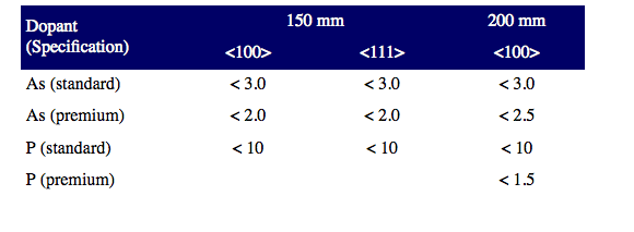
FZ ingots can be intentionally doped through the introduction of gas dopants at the melt interface, or doped later through the Neutron Transmutation Doping (NTD) process in which silicon isotopes Silicon30 are converted in Phosphorous31 leading to an n-type material.
SEH offers both gas-doped and NTD FZ wafers, as well as high resistivity undoped FZ. Diameters up to 200mm.
SEH also offers SOI wafers built with FZ used for the bond and base wafers. These SOI wafers are seeing growing demand for RF/wireless applications.
Gas Doping Process
Float Zone: P-type Crystal
Growth Method: Float Zone single silicon crystal
Type and dopant: P-type (Boron Dopant)
Orientation: <111>, <100>
Float Zone: N-type Crystal
Growth Method: Float Zone single silicon crystal
Type and dopant: N-type (Phosphorous Dopant)
Orientation: <111>, <100>
______________________________
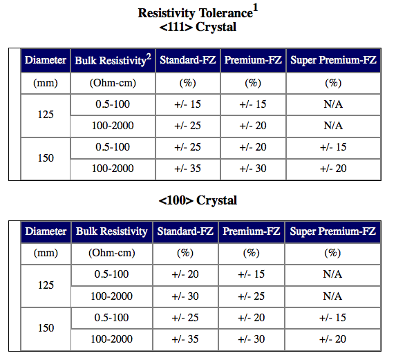
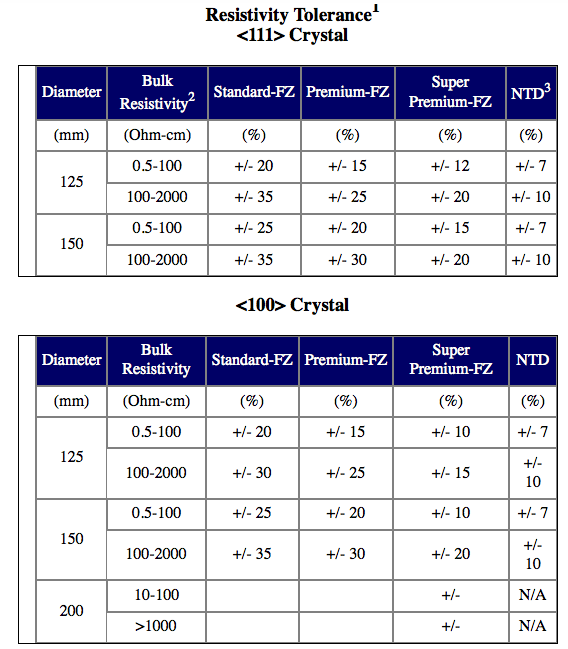
1 This specification table may be subject to change without pre-announcement.
2 Other resistivity ranges such as lower than 0.5 ohm-cm or higher than 2000 ohm-cm are also available. Please contact us for further information.
3 Minimum and maximum resistivity specifications for NTD are 15 ohm-cm and 1000 ohm-cm respectively.
DIFFUSED WAFERS
Silicon wafers with a deep p-n junction created by diffusion techniques are often used for discrete power and MOS power applications, as well as diode based devices. Diffused Wafers are created by diffusing a heavily doped region into a lightly doped wafer. The final thicknesses of both regions can be modified to meet the requirements of the device. Diffused layers are now used more for very high voltage ( > 800V ) Power MOSFET devices. In this application, the
Diffused Wafer (DW) may offer both performance and cost of ownership benefits over EPI wafers having EPI layer thicknesses in excess of 80um.
SEH has more than twenty years of experience manufacturing diffused wafers. The crystal growth and diffusion processes have been optimized to provide the best possible uniformity of both highly and lightly doped regions. Example of DW equivalents to Thick EPI wafers
Example of DW equivalents to Thick EPI wafers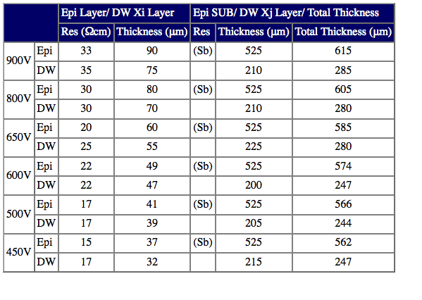
AS SLICED AND AS LAPPED WAFERS
Non polished silicon wafers are used for a variety of discrete and solar cell applications.
The typical process flow for polished silicon wafers is Slicing — Lapping or Grinding — Etching — Polishing.
SEH can supply wafers as sliced (as cut), as lapped, and as etched. The choice will depend on the degree of surface topography and surface damage which may be tolerated by your process. 200mm wafers may be available in As-Sliced, Lapped, or Etched versions. Please inquire.
Example of DW equivalents to Thick EPI wafers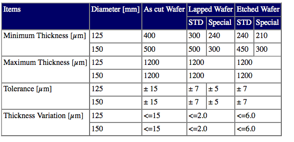
200mm wafers may be available in As-Sliced, Lapped, or Etched versions. Please inquire.
STOCK PRODUCTS
SEH Stock Products are wafers with generic specifications which are typically ready for immediate delivery.
Selected from inventory on-hand, Stock Products offer value and fast response over custom product specifications.
- POLISHED WAFERS
- HIGH RESISTIVITY SUBSTRATE
- EPI WAFER
- MECHANICAL WAFER
- SPV/LIFETIME MONITOR
- P-PARTICLE MONITOR
- SOI WAFER
Other Products – Related Companies
SEH America Affiliates in the Shin-Etsu Group
PVC
ShinTech
Houston, TX (713) 965-0713
https://www.shintechinc.com
Silicones
Shin-Etsu Silicones of America
Akron, OH (800) 544-1754
https://www.shinetsusilicones.com
Photoresists
Shin-Etsu Microsi
Phoenix, AZ (480) 893-8898
https://www.microsi.com/
Synthetic Quartz
Shin-Etsu Quartz Products, Ltd.
https://www.sqp.co.jp/e/
Rare Earth Magnets
Shin-Etsu Magnetics, Inc.
San Jose, CA (408) 383-9240
Lombard, IL (630) 424-3364
https://www.shinetsumagnetics.com